- 您现在的位置:买卖IC网 > Sheet目录224 > ESD7C3.3DT5G (ON Semiconductor)DIODE ESD PROT 3.3V SOT-723
ESD7C, SZESD7C SERIES
Transient Voltage
Suppressors
Micro ? Packaged Diodes for ESD Protection
The ESD7CxxD Series is designed to protect voltage sensitive
1
components from ESD. Excellent clamping capability, low leakage, and
fast response time make these parts ideal for ESD protection on designs
where board space is at a premium. Because of its small size, it is suited
for use in cellular phones, portable devices, digital cameras, power
supplies and many other portable applications.
Specification Features:
? Low Capacitance 6.2 pF to 13 pF
? Low Clamping Voltage
? Small Body Outline Dimensions:
0.047 ″ x 0.047 ″ (1.20 mm x 1.20 mm)
? Low Body Height: 0.020 ″ (0.5 mm)
? Stand ? off Voltage: 3.3 V, 5 V
? Low Leakage
? Response Time < 1 ns
? ESD Rating of Class 3 (> 16 kV) per Human Body Model
? IEC61000 ? 4 ? 2 Level 4 ESD Protection
? SZ Prefix for Automotive and Other Applications Requiring Unique
Site and Control Change Requirements; AEC ? Q101 Qualified and
PPAP Capable
? These are Pb ? Free Devices
Mechanical Characteristics:
http://onsemi.com
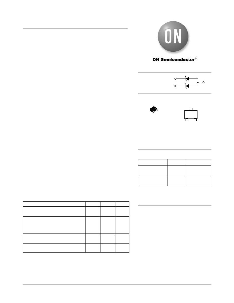
PIN 1. CATHODE 1
2. CATHODE 3
3. ANODE 2
MARKING
DIAGRAM
L5 M
SOT ? 723
CASE 631AA
L5 = Specific Device Code
M = Date Code
*Date Code orientation and/or position may
vary depending upon manufacturing location.
ORDERING INFORMATION
Device Package Shipping ?
CASE: Void-free, transfer-molded, thermosetting plastic
Epoxy Meets UL 94 V ? 0
ESD7CxxDT5G
SOT ? 723
(Pb ? Free)
8000 /
Tape & Reel
LEAD FINISH: 100% Matte Sn (Tin)
MOUNTING POSITION: Any
QUALIFIED MAX REFLOW TEMPERATURE: 260 ° C
Device Meets MSL 1 Requirements
MAXIMUM RATINGS
SZESD7CxxDT5G SOT ? 723 8000 /
(Pb ? Free) Tape & Reel
?For information on tape and reel specifications,
including part orientation and tape sizes, please
refer to our Tape and Reel Packaging Specifications
Brochure, BRD8011/D.
Rating
Symbol
Value
Unit
IEC 61000 ? 4 ? 2 (ESD) Contact
Air
Total Power Dissipation on FR ? 5 Board
(Note 1) @ T A = 25 ° C
Derate above 25 ° C
Thermal Resistance Junction ? to ? Ambient
Junction and Storage Temperature Range
Lead Solder Temperature ? Maximum
(10 Second Duration)
?
P D
R q JA
T J , T stg
T L
± 8.0
± 15
240
1.9
525
? 55 to
+150
260
kV
mW
mW/ ° C
° C/W
° C
° C
DEVICE MARKING INFORMATION
See specific marking information in the device marking
column of the table on page 2 of this data sheet.
Stresses exceeding Maximum Ratings may damage the device. Maximum
Ratings are stress ratings only. Functional operation above the Recommended
Operating Conditions is not implied. Extended exposure to stresses above the
Recommended Operating Conditions may affect device reliability.
1. FR ? 5 = 1.0 x 0.75 x 0.62 in.
See Application Note AND8308/D for further description of survivability specs.
? Semiconductor Components Industries, LLC, 2012
March, 2012 ? Rev. 3
1
Publication Order Number:
ESD7C3.3D/D
发布紧急采购,3分钟左右您将得到回复。
相关PDF资料
ESD7L5.0DT5G
TVS ULT LOW CAP SOT-723
ESD7M5.0DT5G
TVS ESD ULT LOW CAP SOT-723
ESD8V0L2B-03L E6327
TVS LO CAP 2CHAN BIDIR TSLP-3
ESD8V0R1B-02LS E6327
TVS BIDIR 1LINE TSSLP-2-1
ESD9B3.3ST5G
TVS ESD BIDIRECT 300MW SOD-923
ESD9C3.3ST5G
DIODE ESD PROT 3.3V SOD-923
ESD9L3.3ST5G
TVS ESD ULT LOW CAP SOD-923
ESD9M5.0ST5G
IC ESD PROT LO CAP UNIDIR SOD923
相关代理商/技术参数
ESD7C5.0DT5G
功能描述:TVS二极管阵列 ESD PROTECT DIODE RoHS:否 制造商:Littelfuse 极性: 通道:4 Channels 击穿电压: 钳位电压:11.5 V 工作电压:2.5 V 峰值浪涌电流:20 A 安装风格:SMD/SMT 端接类型:SMD/SMT 系列: 最小工作温度:- 40 C 最大工作温度:+ 85 C
ESD7L5.0DT5G
功能描述:TVS二极管阵列 SOT-723 ZENER ESD PBFREE RoHS:否 制造商:Littelfuse 极性: 通道:4 Channels 击穿电压: 钳位电压:11.5 V 工作电压:2.5 V 峰值浪涌电流:20 A 安装风格:SMD/SMT 端接类型:SMD/SMT 系列: 最小工作温度:- 40 C 最大工作温度:+ 85 C
ESD7L5.0DT5G
制造商:ON Semiconductor 功能描述:TVS DIODE 5V SOT-723
ESD7M5.0DT5G
功能描述:TVS二极管阵列 LO CAP ESD PROT 5.0V RoHS:否 制造商:Littelfuse 极性: 通道:4 Channels 击穿电压: 钳位电压:11.5 V 工作电压:2.5 V 峰值浪涌电流:20 A 安装风格:SMD/SMT 端接类型:SMD/SMT 系列: 最小工作温度:- 40 C 最大工作温度:+ 85 C
ESD7V0D5
制造商:MCC 制造商全称:Micro Commercial Components 功能描述:3.3V~12Volts ESD Protection Devices
ESD7V0D5-TP
功能描述:ESD 抑制器 7V 200W
RoHS:否 制造商:STMicroelectronics 通道:8 Channels 击穿电压:8 V 电容:45 pF 端接类型:SMD/SMT 封装 / 箱体:uQFN-16 功率耗散 Pd: 工作温度范围:- 40 C to + 85 C
ESD7V0D9-TP
功能描述:ESD 抑制器 Uni-dir 10mA, 7V RoHS:否 制造商:STMicroelectronics 通道:8 Channels 击穿电压:8 V 电容:45 pF 端接类型:SMD/SMT 封装 / 箱体:uQFN-16 功率耗散 Pd: 工作温度范围:- 40 C to + 85 C
ESD8004MUTAG
制造商:ON Semiconductor 功能描述:LOW CAP ESD PROTECTION - Tape and Reel 制造商:ON Semiconductor 功能描述:REEL / LOW CAP ESD PROTECTION
